A. Scanning Electron Microscope - SEM
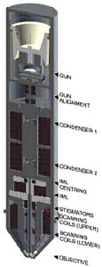 The scanning electron microscope (SEM) is a type of electron microscope that images the sample surface by scanning it with a high-energy beam of electrons in a raster scan pattern. The electrons interact with the atoms that make up the sample producing signals that contain information about the sample's surface topography, composition and other properties such as electrical conductivity.
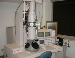
Manufacturer are invited to advertise their product photo free of cost
B. Transmission electron microscopy - TEM
 Transmission electron microscopy (TEM) is a microscopy technique whereby a beam of electrons is transmitted through an ultra thin specimen, interacting with the specimen as it passes through. An image is formed from the interaction of the electrons transmitted through the specimen; the image is magnified and focused onto an imaging device, such as a fluorescent screen, on a layer of photographic film, or to be detected by a sensor such as a CCD camera.
TEMs are capable of imaging at a significantly higher resolution than light microscopes, owing to the small de Broglie wavelength of electrons. This enables the instrument's user to examine fine detail—even as small as a single column of atoms, which is tens of thousands times smaller than the smallest resolvable object in a light microscope. TEM forms a major analysis method in a range of scientific fields, in both physical and biological sciences. TEMs find application in cancer research, virology, materials science as well as pollution and semiconductor research.
Manufacturer are invited to advertise their product photo free of cost
C. Focused ion beam - FIB
Focused ion beam, also known as FIB, is a technique used particularly in the semiconductor and materials science fields for site-specific analysis, deposition, and ablation of materials. An FIB setup is a scientific instrument that resembles a scanning electron microscope (SEM). However, while the SEM uses a focused beam of electrons to image the sample in the chamber, an FIB setup instead uses a focused beam of ions. FIB can also be incorporated in a system with both electron and ion beam columns, allowing the same feature to be investigated using either of the beams. FIB should not be confused with using a beam of focused ions for direct write lithography (such as in proton beam writing), where the material is modified by different mechanisms.
Manufacturer are invited to advertise their product photo free of cost
Note :- Above Photos & Presentation are used for Representation Purpose only not for commercial aspect